

Exp 9. BJT Fixed Bias CE Amplifier
Concept : To demonstrate the working of a BJT Fixed Bias CE Amplifier
Explanation:
A BJT (Bipolar Junction Transistor) amplifier is a type of electronic amplifier that uses bipolar junction transistors to amplify electrical signals. BJTs are three-layer semiconductor devices consisting of an N-type layer (negatively doped), a P-type layer (positively doped), and another N-type layer. There are two main types of BJTs: NPN and PNP.
Working Principle
In a BJT amplifier, the transistor operates in the active region, where the base-emitter junction is forward-biased, and the collector-base junction is reverse-biased. This configuration allows the transistor to amplify the input signal applied to the base, resulting in a larger output signal at the collector12.
Types of BJT Amplifiers
- Common Emitter (CE) Amplifier
- Common Base (CB) Amplifier
- Common Collector (CC) Amplifier
Here we are going to try out the Fixed Bias Common Emitter (CE) Amplifier.
Simulation Mode: Transient
Simulation Parameters: .tran 0.01 10m 0
|
Simulation Type |
Start Time(sec) |
Stop Time(sec) |
Step Time(sec) |
|
.tran |
0 |
10m |
0.01 |
Reference Netlist:
* BJT Fixed Bias CE Amplifier
.model mybjt NPN
V1 COM.1 0 dc 0 ac 1 sin(0 1m 500)
C1 COM.2 COM.1 10u
R1 COM.3 COM.4 22k
R2 COM.3 COM.2 50k
V2 COM.3 0 5
C2 COM.4 COM.5 10u
R3 COM.5 0 100k
Q3 0 COM.2 COM.4 mybjt
.tran 0.01 10m 0
.control
run
plot all
.endc
.end
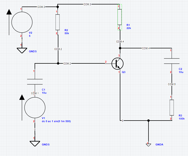
Reference Circuit Schematic:
Make the circuit diagram with the exact pin-to-pin connection as shown below to practice. This will help you to complete the experiment successfully.
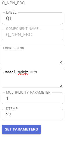
Note: Please check the following parameters of Q1.
Reference Circuit Details:
Supply=COM.3, Input=COM.1 and Output=COM.5
Reference Output:
After the simulation is done, the following output graph appears at the screen showing the voltages and currents across all the nodes.

Conclusion
We can see that the output signal is amplified by almost 60 times. Thus the gain of the amplifier is Vout/Vin=60.
Assignment: Implement a Common Collector(CC) Amplifier using a PNP transistor. Note: Change the NPN to PNP in device parameters.
< Exp 8. Diode Bridge Rectifier with Filter up Exp 10. CMOS Inverter >