
Exp 10. CMOS Inverter
Concept: To demonstrate the working of a CMOS Inverter
Explanation:
A CMOS inverter, or Complementary Metal-Oxide-Semiconductor inverter, is a fundamental building block in digital electronics. It is widely used in memory chips, microprocessors, and other integrated circuits. Here’s a brief overview:
How It Works
A CMOS inverter consists of two types of transistors: NMOS (n-type metal-oxide-semiconductor) and PMOS (p-type metal-oxide-semiconductor). These transistors are connected in series between the power supply (VDD) and ground (GND). The input signal is applied to the gates of both transistors, and the output is taken from the connection between them.
When the input is low (0): The NMOS transistor is off, and the PMOS transistor is on, resulting in a high output (1).
When the input is high (1): The NMOS transistor is on, and the PMOS transistor is off, resulting in a low output (0).
Simulation Mode: Transient
Simulation Parameters: .tran 0.1m 10m 0 UIC
|
Simulation Type |
Start Time(sec) |
Stop Time(sec) |
Step Time(sec) |
|
.tran |
0 |
10m |
0.1m |
Reference Netlist:
* CMOS Inverter
.model mymosfet NMOS
.model mymosfet2 PMOS
M1 COM.1 COM.2 0 0 mymosfet
M2 COM.1 COM.2 COM.3 COM.3 mymosfet2
V1 COM.2 0 PULSE(0 5 1u 1u 1u 1m 2m 0.0 )
V2 COM.3 0 DC 5
.tran 0.1m 10m 0 UIC
.control
run
plot all
.endc
.end
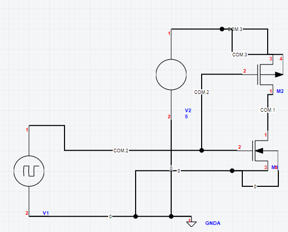
Reference Circuit Schematic:
Make the circuit diagram with the exact pin-to-pin connection as shown below to practice. This will help you to complete the experiment successfully.
Note: Please change the following parameter for M2 from ".model mymosfet NMOS" to ".model mymosfet2 PMOS".


Reference Circuit Details:
Supply= COM.3 Input=COM.2 and Output=COM.1
Reference Output:
After the simulation is done, the following output graph appears at the screen showing the voltages and currents across all the nodes.
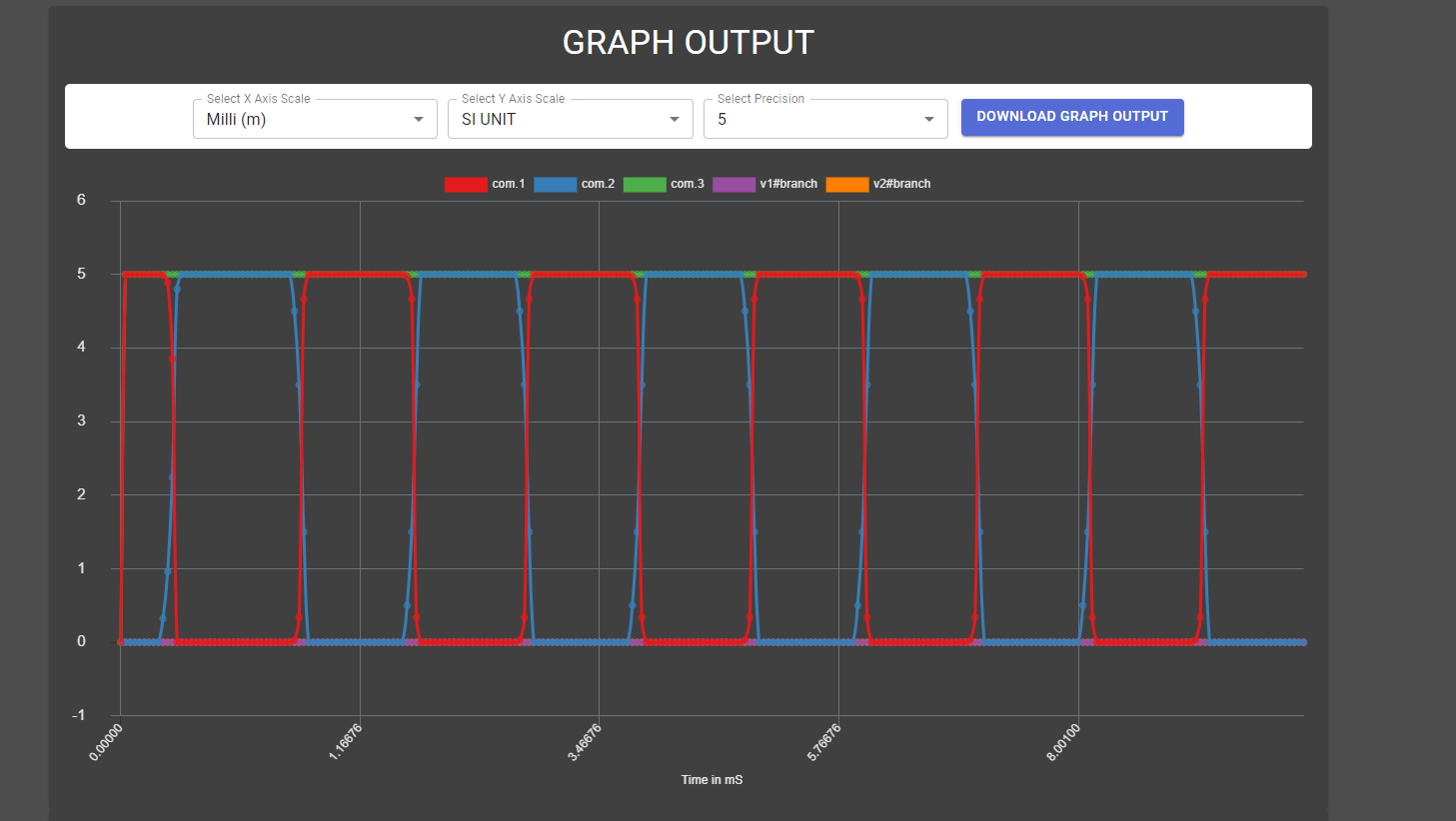
Conclusion
The output demonstrates the working of a CMOS inverter where the output is exactly the inverted form of the input.
Assignment:
Implement a CMOS pass transistor.